Supplementary Notes on Circuit Analysis
David A. Torrey
Show all articles by Prof. David Torrey
Clarkson University, Capital Region Campus
80 Nott Terrace
Schenectady, NY 12308
[email protected]
Circuit Components

Circuit Analysis
Additional Info
Overview
The following notes are offered to help you refresh your memory on some fundamental circuit analysis techniques. In particular, a review of reactive components and transformers is offered, followed by a brief review of time domain circuit analysis. The notes conclude with a discussion of some basic power concepts. The orientation of these notes is from the perspective of the power electronics engineer. That is, while these notes should not present you with any new material (I hope!), they may present things in a way which is different from the treatment given in an introductory circuits text. These notes are not intended to provide an exhaustive treatment of circuit analysis; see [1, 2] for a more complete treatment.
Circuit Analysis
This semester we are going to be analyzing circuits in the time domain. There are three reasons for this. First, it is a nuisance and time-consuming to be working with Laplace transforms. Second, Laplace transforms provide limited insight into how a circuit behaves. Third, we are not going to deal with anything more complex than second-order circuits, so the analysis is rather straight-forward.
Because one element of solving a differential equation involves determining a particular solution, we are also going to briefly discuss phasor analysis. Since phasor analysis gives us a steady state solution for a network which is excited at a particular frequency, we can exploit phasor analysis to quickly give us the particular solution. You may recall that the particular solution and the steady state solution are just different names for the same thing.
Time Domain Transient Analysis
This section provides a brief review of circuit analysis in the time domain. Specifically, we are going to walk through the process of analyzing the snubber circuit shown in Fig. 5 as the circuit moves through two of its topologies. This circuit is chosen for two reasons. First, we are going to study this circuit in considerable detail near the end of the semester, and you will get more out of that discussion if you follow the analysis presented here. Second, this circuit gives a practical example of a circuit with a second-order response.
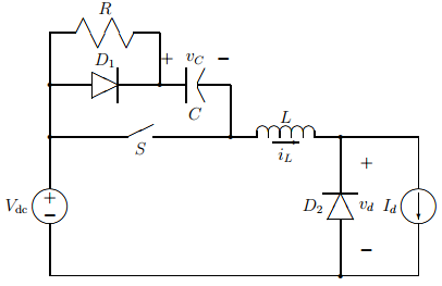
Figure 5 - A combined turn-on and turn-off snubber.
The snubber circuit given in Fig. 5 is comprised of the resistor $R$, the diode $D_1$, the capacitor $C$ and the inductor $L$. The function of these elements is to shape the current through the switch $S$ at turn on and to shape the voltage across the switch at turn-off. Proper shaping of the current and voltage is necessary to keep the switch within its safe operating area. We are going to focus on two of the four topologies that the circuit moves through when the switch is turned off.
Briefly, the way the snubber circuit operates at turn-off is as follows. When the switch opens, the inductor (and load) current $I_d$ is transferred to diode $D_1$ and the capacitor. The constant current through the capacitor forces $v_C$ to ramp linearly; recall Eq. 4. During this time there is zero voltage across the inductor since the current through it is constant. When $v_C = V_{dc}$, diode $D_2$ begins conducting, forcing $v_d = 0$. With diode $D_2$ available for picking up the load current, $L$ and $C$ now begin to ring (or resonate). By the time $i_L$ reaches zero, $v_C > V_{dc}$. When $i_L = 0$, diode $D_1$ opens, and we move into a topology which places $R$, $L$, and $C$ in series.
Let us now consider the topologies where $L$ and $C$ ring and where $R$, $L$ and $C$ are in series more carefully in order to more rigorously describe circuit operation.
$L$ and $C$ Ringing
Define $t=0$ to be the time when diode $D_2$ turns on, thereby setting $L$ and $C$ free to ring. The active circuit topology is shown in Fig. 6. Our initial conditions are:
| $$\begin{eqnarray} i_L(0) & = & I_d \label{eq:lcic1} \\ \nonumber v_C(0) & = & V_{dc} \quad. \end{eqnarray}$$ | (25) |
Because we have a second-order system, we are also going to find it useful to determine the time rates of change of $i_L$ and $v_C$ at $t=0$. Using the methods identified in Sec. 1, we have:
| $$\begin{eqnarray} \left. \frac{di_L}{dt} \right|_{t=0} & = & 0 \label{eq:lcic2} \\ \left. \frac{dv_C}{dt} \right|_{t=0} & = & \frac{I_d}{C} \nonumber \quad. \end{eqnarray}$$ | (26) |
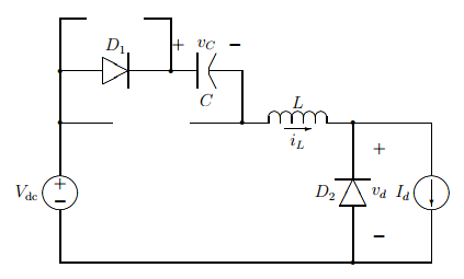
Figure 6 - The active snubber topology while L and C are ringing.
We are interested in the capacitor voltage and the inductor current, since these dictate the maximum switch voltage and the time when diode $D_1$ turns off, respectively. Let's start with the inductor current. Recognizing that the capacitor current and the inductor current are the same while we are in this topology, applying Kirchhoff's voltage law gives
| $$L \frac{di_L}{dt} + \frac{1}{C} \int i_L \, dt = V_{dc} \quad.$$ | (27) |
Differentiating Eq. 27 once with respect to time to get rid of the integral sign gives our second order differential equation:
| $$\frac{d^2i_L}{dt^2} + \frac{1}{LC} i_L = 0 \quad.$$ | (28) |
The general response for this form of second-order constant-coefficient differential equation is
| $$i_L = A \cos \omega_0 t + B \sin \omega_0 t \: ; \quad \omega_0 = \frac{1}{\sqrt{LC}} \quad.$$ | (29) |
We need to apply our initial conditions in order to solve for $A$ and $B$. Using Eqs. 25 and 26 gives
| $$\begin{eqnarray} I_d & = & A \\ \nonumber 0 & = & B \omega_0 \quad, \end{eqnarray}$$ | (30) |
which leads us to conclude that
| $$i_L = I_d \cos \omega_0 t \quad.$$ | (31) |
To find the capacitor voltage we can do one of two things. We could write a second order differential equation in terms of $v_C$, or we could use Eq. 4. In this case applying Eq. 4 appears to be the easiest route.
| $$v_C(t) = V_{dc} + \frac{1}{C} \int_0^t I_d \cos \omega_0 t \,dt \quad.$$ | (32) |
This reduces to
| $$v_C(t) = V_{dc} +\sqrt{ \frac{L}{C} } I_d \sin \omega_0 t \quad.$$ | (33) |
Equation 31 indicates that the inductor current rings down to zero immediately after diode $D_2$ turns on. Equation 33 shows that the capacitor voltage increases by an amount which is dictated by the energy which is stored in the inductor when $D_2$ turns on.
$R$, $L$ and $C$ in Series
When the inductor current rings down to zero, diode $D_1$ opens. Because $v_C > V_{dc}$, the excess potential forces some current to flow back to the source. The current going back to the source now flows through the series combination of $R$, $L$ and $C$. The time $t_1$ when the inductor current reaches zero is found by looking at Eq. 31:
| $$t_1 = \frac{\pi}{2 \omega_0} \quad.$$ | (34) |
The active topology we are now considering is shown in Fig. 7. Our initial conditions on entering this topology are
| $$\begin{eqnarray} i_L(t_1) & = & 0 \\ \nonumber v_C(t_1) & = & V_{dc} + \sqrt{ \frac{L}{C} } I_d \quad. \label{eq:rlcic1} \end{eqnarray}$$ | (35) |
Our initial conditions on the first derivatives of $i_L$ and $v_C$ are
| $$\begin{eqnarray} \left. \frac{di_L}{dt} \right|_{t=t_1} & = & -\omega_0 I_d \\ \nonumber \left. \frac{dv_C}{dt} \right|_{t=t_1} & = & 0 \quad. \label{eq:rlcic2} \end{eqnarray}$$ | (36) |
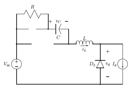
Figure 7 - The active snubber topology when R, L and C are in series.
Applying KVL around the snubber loop gives
| $$L \frac{di_L}{dt} + Ri_L + \frac{1}{C} \int i_L \, dt = V_{dc} \quad.$$ | (37) |
Differentiating once with respect to time gets rid of the integral term:
| $$\frac{d^2i_L}{dt^2} + \frac{R}{L} \frac{di_L}{dt} + \frac{1}{LC} i_L = 0 \quad.$$ | (38) |
We are now faced with a more complicated differential equation, due to the presence of the resistor.
If we assume a solution of the form $i_L = A e^{s(t-t_1)}$, upon substituting this into Eq. 38 we get
| $$\left\{ s^2 + \frac{R}{L} s + \frac{1}{LC} \right\} A e^{s(t- t_1)} = 0 \quad.$$ | (39) |
It follows that in order for our assumed solution to be valid $s$ must satisfy the characteristic equation
| $$s^2 + \frac{R}{L} s + \frac{1}{LC} = 0 \quad.$$ | (40) |
The roots of the characteristic equation are
| $$s_{1,2} = - \frac{R}{2L} \pm \sqrt{ \left[ \frac{R}{2L} \right]^2 - \frac{1}{LC} } = - \alpha \pm \sqrt{ \alpha^2 - \omega_0^2} \quad.$$ | (41) |
There are three possible outcomes for the two roots of the characteristic equation:
- $s_1$ and $s_2$ could be real and distinct. ($\alpha^2 > \omega_0^2$.)
- $s_1$ and $s_2$ could be real and the same (repeated). ($\alpha^2 = \omega_0^2$.)
- $s_1$ and $s_2$ could be complex conjugates. ($\alpha^2 < \omega_0^2$.)
These three cases represent over-, critically-, and under-damped responses, respectively. The appropriate forms of the solution for $i_L$ corresponding to these three cases are summarized in Table 1.
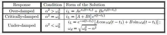
Table 1 - A summary of the three possible responses for $i_L$.
We really cannot determine which of the three solutions we must choose until the element values are known. From experience, a practical combination of snubbing element values will usually lead to an over-damped response, so this is the one with which we will work. The other cases simply involve slightly different algebra.
Applying our initial conditions to the assumed over-damped solution gives
| $$\begin{eqnarray} 0 & = & A + B \\ \nonumber -\omega_0 I_d & = & As_1 + B s_2 \quad. \end{eqnarray}$$ | (42) |
Solving for $A$ and $B$ gives the inductor current to be
| $$i_L(t) = \frac{\omega_0 I_d}{s_2 - s_1} \left[ e^{s_1(t-t_1)} - e^{s_2(t-t_1)} \right] \quad.$$ | (43) |
Finding $v_C$ is a little more tedious. Using the approach we used before, we put Eq. 43 into Eq. 4:
| $$v_C(t) = V_{dc} + \sqrt{ \frac{L}{C} } I_d + \frac{1}{C} \int_{t_1}^t \left\{ \frac{\omega_0 I_d}{s_2 - s_1} \left[ e^{s_1(t-t_1)} - e^{s_2(t-t_1)} \right] \right\} \, dt \quad.$$ | (44) |
Performing the indicated integration and reducing gives
| $$v_C(t) = V_{dc} + \frac{\omega_0 I_d}{C(s_2 - s_1)} \left[ \frac{e^{s_1(t-t_1)}}{s_1} - \frac{e^{s_2(t-t_1)}}{s_2} \right] \quad.$$ | (45) |
It can be verified by inspection that $i_L$ returns to zero and $v_C$ returns to $V_{dc}$ after a long time, suggesting that we have not made any obvious blunders in our analysis.
Steady State (Phasor) Analysis
It was relatively straight-forward to determine the particular (steady state) response which was associated with the differential equations in the snubber example considered in the last subsection. This is because only dc quantities were involved. When ac quantities are involved, drawing on phasor analysis can save us a lot of effort (and algebra!).
Consider the simple rectifier circuit shown in Fig. 8. This circuit uses a freewheeling diode so that when the source voltage is negative, $v_d = 0$. When the source voltage is positive, $v_d = V_s \sin \omega t$. What we would like to do is describe the load current $i_d$ during operation of the circuit. Here, we are only going to proceed to the point where we have made use of phasor analysis to help us determine the particular solution for the load current during the positive half cycle of the source.
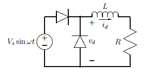
Figure 8 - A half-wave rectifier with freewheeling diode.
During the positive half cycle of the source voltage, the load current is dictated by the differential equation
| $$L\frac{di_d}{dt} + R i_d = V_s \sin \omega t \quad.$$ | (46) |
The homogeneous (natural) solution to Eq. 46 is $i_{d,h} = A e^{-Rt/L}$; the constant $A$ is chosen to satisfy the initial condition on $i_d$. The particular solution is a little more complicated.
We have a couple of options open to us when trying to find the particular solution. We could assume a response of the form
| $$i_{d,p} = A \sin (\omega t - \phi)$$ | (47) |
and plug this into the differential equation and solve for $A$ and $\phi$. We could also use phasor analysis.
If we recall that
| $$\sin \omega t = \Im \left\{ e^{j\omega t} \right\} \quad,$$ | (48) |
and
| $$\frac{d}{dt} \Im \left\{ e^{j\omega t} \right\} = \Im \left\{ j\omega e^{j\omega t} \right\} \quad,$$ | (49) |
then we can assume that the particular response of the current satisfies
| $$i_{d,p} = \Im \left\{ \hat{I} e^{j\omega t} \right\} \quad,$$ | (50) |
where $\hat{I}$ could be complex. (The symbol $\Im\left\{\mbox{ }\right\}$ denotes the imaginary part of what is enclosed in the brackets.) Using this information, our differential equation reduces to
| $$\left[ j\omega L + R \right] \hat{I} e^{j\omega t} = V_s e^{j\omega t} \quad,$$ | (51) |
where it has been suppressed that we are interested in the imaginary component of each term. Our willingness to work with complex numbers has reduced our differential equation to a complex algebraic equation.
When you were first introduced to phasor analysis, you probably worked with the real part of the complex solution. The real part works fine when the forcing function is a cosine, but it creates excess baggage in the form of a constant phase shift when the forcing function is a sine. Using the imaginary part of the complex solution eliminates this excess baggage.
Solving Eq. 51 for $\hat{I}$ gives
| $$\hat{I} = \frac{V_s}{\sqrt{R^2 + (\omega L)^2}} e^{-j \phi}; \quad \phi = \tan^{-1} \frac{\omega L}{R} \quad.$$ | (52) |
Putting Eq. 52 into Eq. 50 gives
| $$i_{d,p} = \frac{V_s}{\sqrt{R^2 + (\omega L)^2}} \sin (\omega t - \phi) \quad.$$ | (53) |
It may not be clear that the phasor approach is simpler than the substitution and algebraic manipulation required with the solution given in Eq. 47. With a little practice, it should be possible for you to perform the phasor analysis associated with this problem in your head, thereby making the phasor approach much faster.
Basic Power Concepts
In power electronics, we are concerned about the conversion of electrical energy between various forms. People often come out of a first course in circuit analysis without either having had a thorough discussion of power concepts, or with some misconceptions. This section briefly addresses some basic power concepts, with emphasis on the way we are often going to consider energy flow.
To begin, the instantaneous power is given by the product of voltage and current:
| $$p_1(t) = v_1(t) i_1(t) \quad.$$ | (54) |
The average power is determined in the same way that the average voltage or current is determined. That is,
| $$\langle p_1(t) \rangle = P_1 = \frac{1}{T} \int p_1(t) \,dt \quad.$$ | (55) |
Note that the average power is not given by the product of the average voltage and the average current. In other words, the average of the product does not equal the product of the averages. If you do not see this from Eqs. 54 and 55, consider a resistor connected across a sinusoidal voltage source. The average voltage across the resistor is zero, the average current through the resistor is zero, but the average power consumed by the resistor is not zero.
A consequence of Eq. 55 is that if a frequency component of $v_1(t)$ is to contribute to the average power, then that frequency component must also be present in $i_1(t)$. This observation is integrally tied to the concept of signal orthogonality; see [4] for additional details about orthogonality. The usefulness of this concept is significant. We will sometimes use it to dramatically reduce the amount of analysis we must perform in order to determine the average power flow in a circuit.
Inductors and capacitors do not consume average power in the periodic steady state. They do, however, consume instantaneous power. This instantaneous power represents the flow of energy, specifically the time rate of change in stored energy. Consider the case of an inductor. The energy stored in an inductor is
| $$\begin{eqnarray} w(t) & = & w(0) + \int_0^t p(t')\,dt' \nonumber \\ & = & w(0) + \int_0^t \left[ L\frac{di}{dt'} i(t') \right] \, dt' \nonumber \\ & = & w(0) + \int_0^t \frac{d}{dt'} \left[ \frac{1}{2} L i^2(t') \right] \, dt' \nonumber \\ & = & w(0) + \frac{1}{2} L i^2(t) - \frac{1}{2} L i^2(0) \nonumber \\ w(t) & = & \frac{1}{2} L i^2(t) \quad. \end{eqnarray}$$ | (56) |
The distinction between energy and power flow is important in power electronics. This is because it is through the utilization of energy storage components that we can alter the instantaneous power spectra at the output of the converter from the instantaneous power spectra at the input of the converter. Further, by exploiting the conservation of instantaneous power, average power, and energy flow, we are able to not only gain additional insights into the operation of a converter, but to do so with less cumbersome analysis.
Summary
These notes have presented a brief discussion of some of the circuit components we will be using this semester. A brief review of time domain circuit analysis techniques was presented, followed by a discussion of some basic power concepts. These notes were not intended to be a substitute for a circuit analysis course; they were intended to help orient you in the way a power electronics engineer approaches the analysis of a circuit.
The concepts presented here must be mastered before any power electronic converters can be understood. This material has been presented so that we may focus on the deeper issues of power electronics, not circuit analysis techniques.
References
- J. W. Nilsson, Electric Circuits, $3^{\rm rd}$ Ed., Addison-Wesley, 1990.
- D. E. Johnson, J. R. Johnson and J. L. Hilburn, Electric Circuit Analysis, Prentice-Hall, 1989.
- J. G. Kassakian, M. F. Schlecht and G. C. Verghese, Principles of Power Electronics, Addison-Wesley, 1991.
- D. A. Torrey, ``Supplementary notes on signal analysis,'' Course 34-408, Rensselaer Polytechnic Institute, 1994.
Change log
2/20/2019
- Initial article release.